
“According to a research conducted by Collett International Research Inc., one in five chips fails because of the signal integrity.”
In this article, we will discuss a very important issue of VLSI design called signal integrity and crosstalk which are responsible for the failure of many ASICs now a day. We will discuss signal integrity and crosstalk in this article. The effects of crosstalk and prevention techniques will be discussed in the next two articles.
Signal Integrity:
Signal could be defined as information in the form of wave/impulse which is used for communication between two points. In Digital form, it is either in state 1 (high) or in state 0 ( Low) as shown in the figure-1 below.
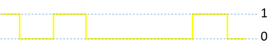 |
| Figure-1: Digital signal |
By definition integrity means “complete or unimpaired”. Or We can say that maintaining the actual form of anything over time without any distortion.
So signal Integrity could be defined as replication of the entire signal while transmitting from one point to another without any distortion in its quality. Or In a broader perspective, we can say that Signal Integrity is the ability of an electrical signal to carry information reliably and resist the effects of high-frequency electromagnetic interference from nearby signals.
Signal Integrity addresses two concerns in digital design
•Timing of signal – Does the signal reach the destination when it is supposed to?
•Quality of signal – When the signal reaches, is it in good condition?
“Timing” is everything in high-speed digital design.
“Timing” is everything in high-speed digital design.
So the goal of Signal Integrity is to ensure reliable, high-speed data transmission from one point to another point inside the chip through the metal lines. Increased data rate and lower technology node, Maintaining signal integrity is a big challenge.
In a nutshell, if the signal travels through a net without any distortion, Signal Integrity is high, If there are lots of noise added on it / distortion occur/delay occurred, Signal Integrity is less.
Signal Integrity may be affected by various reasons, but major reasons are:
In next section we will discuss Crosstalk issue.
What is Crosstalk?
Crosstalk could be defined as a phenomenon in which logic transmitted in one net creates undesired effects on its neighbouring nets. Or in another world, we can say switching of a signal in one net can interfere in the neighbouring net, which is called crosstalk.
When a signal switches, it may affect the voltage waveform of a neighbouring net. The switching net is typically identified as the “aggressor” and the affected net is the “victim.” Figure-2 shows a typical arrangement of aggressor and victim net.
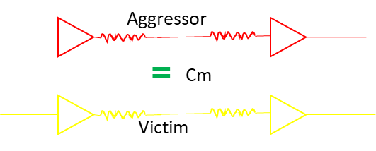 |
| Figure-2: Aggressor and Victim nets |
Crosstalk is a very severe effect especially in lower technology node and high-speed circuitsand it could be one of the main reason of chip failure. In the next section, we would discuss the crosstalk mechanism in VLSI Design.
Crosstalk mechanism
Crosstalk occurs via two mechanisms:
- Inductive Crosstalk
- Electrostatic crosstalk
Electrostatic crosstalk occurs due to mutual capacitance between two nets. The electric voltage in a net creates an electric field around it. If the electric field is changing, It can either radiate the Radio waves or can couple capacitively to the adjacent net. Such coupling of the electric field is called electrostatic crosstalk.
Out of two mechanisms explained here, Electrostatic Crosstalk mechanism is more significant and problematic than Inductive crosstalk. So in this section, we will talk about Electrostatic crosstalk.
Parasitic capacitances related to Interconnects
The main reason of crosstalk is the capacitance between the interconnects. So in this section, we will investigate various capacitance associated with metal interconnects. Figure-3 shows the various parasitic capacitances get formed inside an ASIC (click on image for a better view).
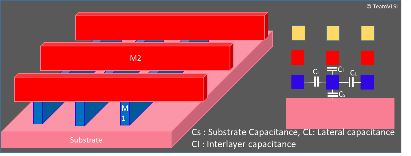 |
| Figure-3: Various capacitances associated with interconnects |
After the FEOL (Front Line Of Line) fabrication, a thick SiO2 insulating layer is deposited all over the substrate before metal-1 (M1) layer fabrication. The insulating layer between M1 and substrate acts as a dielectric and forms a capacitance between M1 and substrate. this is called substrate capacitance (cs). M1 is patterned and the unwanted metal areas are etched away and again empty regions are filled with SiO2. So there is the formation of parasitic capacitance between two neighbouring M1 nets (same metal layers) which is called lateral capacitance (CL). M2 layer is fabricated above M1 followed by SiO2 layer. So there is the formation of interlayer capacitance (CI) between any two conjugative metal layers. Interlayer capacitance can be formed not only conjugative metals but also the metals far away to each other, like M2-M4 or M2-M5. The value of all these capacitance depends on two factors, common area and the gap between them. These capacitances are directly proportional to the common area between them and inversely proportional to the gap between them.
Summary
This article explained the signal integrity, crosstalk, crosstalk mechanisms and parasitic capacitances related to interconnects. The effects of crosstalk are crosstalk glitch or crosstalk noise and crosstalk delay or delta delay. In the next article, we will discuss crosstalk glitch and crosstalk delay.
Thank you.
very informative article.
Thank you.
Happy learning!!!