In the last article, we discussed the antenna violation. How do antenna violations occur, and what is the mechanism to occur antenna effect or Plasma Induced Gate oxide damage. So in this article, we will discuss the solution part of the antenna effect, which is how to prevent the antenna violations.
How to prevent antenna violation?
Before discussing the prevention, let’s recall the root cause of the antenna effect, and then it will be easy to understand the prevention techniques. The antenna effect occurs mainly due to the excessive accumulation of charges on a metal interconnect connected to the gate of transistors during the plasma etching of the metal interconnect. The amount of accumulated charge depends on the area of the metal interconnect connected to the gate. The excessive accumulated charges get discharged through the thin gate oxide and it causes permanent damage to the gate oxide.
Based on the above-mentioned reason for antenna violation, the following three approaches can be applied to prevent the issue. The first method is to reduce the amount of charge accumulation and this can be achieved by reducing the area of metal interconnect connected to the gate of a transistor. The second method is to increase the gate area so the ratio (metal area)/(gate area) becomes lesser than the permitted maximum metal to gate area ratio. This can be achieved by attaching the floating gates to the related net. The third method is to provide an alternative path to get discharge the accumulated charges on the gate of the transistor which is the addition of an antenna diode.
Three basic techniques are to prevent antenna violations are:
- Metal hopping
- Floating gate attachment
- Antenna diode
Now it’s important to know about antenna rules and violations. We will come back to this point after seeing the antenna rules.
Antenna Rules
A process design kit (PDK) comes with some rules deck files. The antenna rule set is a part of the rule deck. All the rule set must be checked before the tapeout. In antenna rules, the most common rule is the antenna ratio.
- Antenna ratio is the ratio of the metal area connected to the gate to the total area of the gate
- Antenna ratio is defined in the following form:
Antenna area / Gate area < Maximum antenna ratio
Example of antenna rule violation
Consider three cases here:
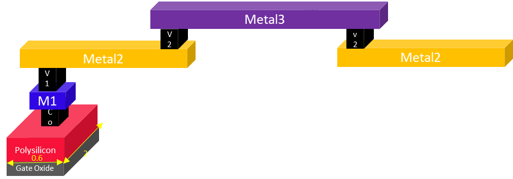
In case-1 suppose metal-2 has length = 200um as shown in the above figure and width of metal =1um. This metal wire is connected to the gate of a transistor. The transistor is having gate width = 2um and length = 0.6um.
Therefore, Total metal area = 200×1 = 200um^2
Total gate area = 0.6 x 2 = 1.2um^2
Therefore, antenna ration = 200/1.2 = 166.2
In case-2 suppose the situation is same but the metal-2 is connected to 4 such transistors instead of 1.
Therefore, Total metal area = 200×1 = 200um^2
Total gate area = 0.6 x 2 x 4= 4.8um^2
Therefore, antenna ration = 200/4.8 = 41.66
In case-3 suppose the metal-2 is broken into two parts of 50um each and connected through metal-3 as shown in the figure below. Such a connection is called metal hoping.
Now, Total metal-2 area = (50×1)x2 = 100 um^2
Total gate area = 0.6 x 2 = 1.2 um^2
Therefore, antenna ration = 100/1.2 = 83.33
Suppose the antenna ratio is given 100 in the antenna rule. So out of the three cases above explained, Case 1 is violating the antenna rule and case 2 and case 3 is not violating the antenna rule.
How to fix the antenna violations
Above example shows that If we increase the gate area by increasing the number of connected transistors, it will reduce the antenna ratio. Another approach could be by reducing the antenna area, that breaks the metal and insert the jumper in between. So we can reduce the antenna ratio in two ways:
- Reduce the antenna area – Jumper insertion or metal hoping
- Increase the gate area – by dummy transistor insertion
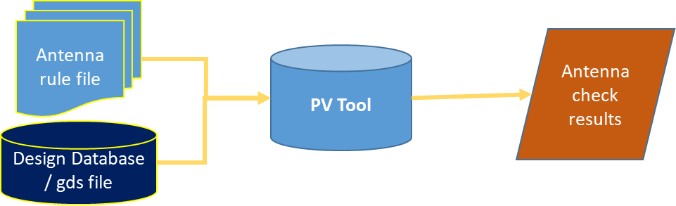
Antenna Checks (Physical Verification)
- Antenna checks verify the layout against the antenna rules of rule decks. There are many more checks need to perform before tapeout like DRC, ERC, LVS etc and these all are collectively called physical verification of layout.
- Physical verification tools (like Calibre, Assura, IC Validator) varifies the antenna rule for all the layers for which antenna rule is applicable.
- Antenna rules strongly depend on the process nodes.
Fixes of antenna violation
1. Jumper Insertion or Metal hoping
Best way to break the lengthy metal into small pieces and using jumpers route them through other metal layers as shown in the above figure (click on the image see the large image). This process is called jumper insertion of metal hoping.
2. Dummy transistor insertion
The effective gate area can be increased by inserting dummy transistors as shown in the above figure. This will decrease the antenna ratio and help to meet to antenna rule. In a practical scenario, we can add a floating inverter/buffer. We attach the input of buffer/Inverter to the concerned net and leave the output floating. This will increase the effective gate area and help to overcome the antenna violation.
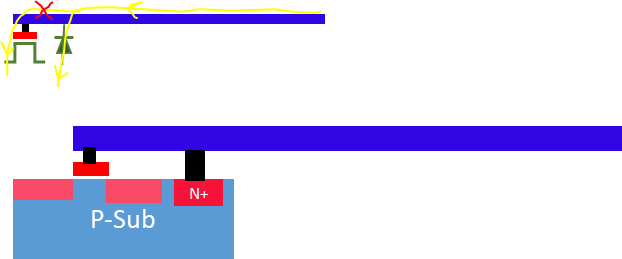
3. Antenna diode insertion
• Antenna diode -Reverse biased
• Placement location – Near the gate terminal
• Plasma etching 400-800 degree Celsius
• High Temperature – Diode is thermally unstable
• During plasma etching – Reverse saturation region
• At reverse saturation region – like a resistive path
• Normal operation -40 to 125 degree Celsius
• Standard cell – Antenna diode cell
• Single terminal standard cell, N+ on Psub.
Various techniques for antenna prevention have been explained in this article. I tried to explain these in the simplest way and hope you are able to understand these thoroughly.
Thank you.


Why antenna diode to be placed near gate,if it is placed far way also it will discharge right? (or) Antenna diode to be palced at input side or outputside?why?
What is the functionality of antenna diode after discharged,does it also manufacture?
Please answer,these were asked in my interview
Hi Mallikarjun,
1. our focus is to prevent the gate oxide and placing the antenna diode near gate is the choice. Placement of antenna diode far from gate cloud lead a high resistive path and that case our gate might not be protected.
2. Yes, It is always there as it is created in base layer. But since it is reverse connected so it remain idle.
During etching the electro static charge gets accumulated along the metal wire and you can imagine this as a distributed voltage source . Now in order to protect the gate from these currents the diode needs to be close to the gate where the antenna is failing.
Imagine that you have placed the diode far away from the gate , Now the Charge accumulated on the metal wires between the gate and the inserted diode can potentially damage the gate.
Hope this helps!
Thank You.
formula to calculate antenna ratio remain same or it varies with change in technology node???