Gate Oxide of a MOS transistor is the most sensitive part of a MOS device. Special care needs to be taken during fabrication of ASIC to protect it from any damages during fabrication steps and ASIC operation too. The antenna effect is a phenomenon that may cause damage to the gate oxide of MOS during the fabrication process especially due to the plasma etching process. In this article, we will investigate the antenna effect phenomena in detail and the reasons which are responsible for this effect.
What is the Antenna Effect?
The term Antenna Effect might not give you the right intuition about the actual effect it may lead you to think about electromagnetic radiation or transmitter-receiver concepts but here the case is different. So It has another popular name which is called “Plasma Induced Gate Oxide Damage” which provides the right intuition about the effect. As this name itself indicates that this is an effect caused by the Gate Oxide Damage due to the Plasma Etching process during the fabrication process of VLSI chips.
Although the antenna effect occurs during the fabrication stage of the chip especially at the time of plasma etching but the prevention mechanism should be set in the physical design stage. The fabrication laboratory provides the antenna rule file which must be checked and designed should be cleaned as per the antenna rule during the physical signoff stage.
In fabrication flow first FEOL (Front End Of Line) is fabricated which involves the fabrication of all MOS transistors. Once the FEOL fabrication is done BEOL (Back End Of Line) fabrication starts which involves the fabrication of metal interconnects. Antenna effect comes into the picture while BEOL fabrication.
In IC manufacturing process Plasma etching process is used to fabricate the metal interconnects. Plasma etching is a dry and anisotropic etching process, used for selective etching. Plasma contains high energetic ions and radicals which get collected by the metal interconnects while the etching process of metals. Figure-1 shows the structure of MOS and collection of plasma by the interconnect.
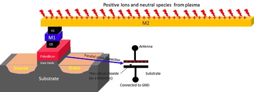 |
| Figure-1: MOS structure and plasma etching |
The amount of charge accumulation depends on the surface area of interconnect. These collected ions increase the potential of the interconnect and if the interconnect is connected to the poly gate, ultimately the potential of the gate will increase. Due to this increased potential of the gate, a drainage path may be formed through the gate oxide to substrate to balance this extra accumulated charge on the gate. If the amount of charge accumulation is high, this drainage path through the gate oxide may either breakdown the gate oxide which leads to permanent damage of MOSFET or may create charge trapping in the gate oxide which further leads to many side effects like early gate oxide breakdown, mobility degradation and threshold voltage shift.
Gate oxide damage occurs basically due to plasma etching of interconnects connected to the gate, that’s why this effect is also called “Plasma Induced Gate Oxide Damage” or “Antenna Effect”. The metal interconnect which collects the plasma (ions) and is connected to the gate is basically termed as the antenna. Here it is important to know the fabrication process of interconnects which is explained in the next section.
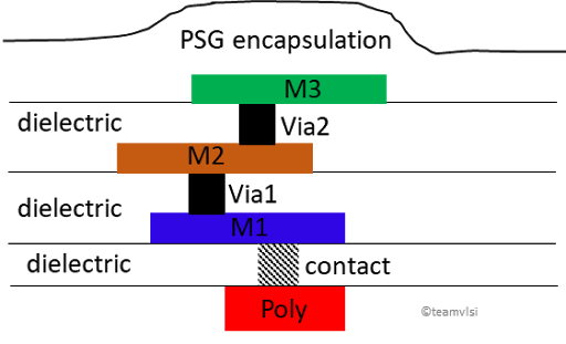
Over the polysilicon, a layer of dielectric is deposited and then cuts are made for the contact. Over the contact, Metal-1 is deposited and patterned and etched the extra metal and filled the whole region by the dielectric. Now before fabricating the metal-2, cuts are made in dielectrics for Via-1 and filled with Via-1 then over the via-1 Metal-2 is deposited. Again in the same way Metal 2 is etched and filled with dielectrics. This process is repeated as many times as the number of metal layers is there. At the end of all the metals processed, A PSG encapsulation is done as shown in the figure.
There are basically three steps are performed to process any metal layer after the corresponding via/contact is fabricated.
- Deposition
- Etching
- CMP
In the first step metal is deposited, In the second step the unwanted area of metal is etched away and in the third step, CMP (Chemical Mechanical Policing) is done.
Now let’s talk more about the etching process. There are basically two types of etching processes is there, one is called wet etching with chemicals and the second is a dry etching with gasses. Dry etching provides complete anisotropic etching in which the lateral etching rate is zero. The most popular plasma etching is a dry etching process which is explained in brief in the next section.
Plasma Etching
Here the plasma etching process will be explained in brief just to understand the process. Plasma etching involves a high-speed stream of plasma of an appropriate gas mixture being shot at the sample. The plasma source is known as etch species are either charged ions or neutral atoms or radicals. During the etching process, plasma generates volatile etch products from the chemical reaction between the target material and the reactive species generated by the plasma. A basic setup of plasma etching has shown in the figure below.
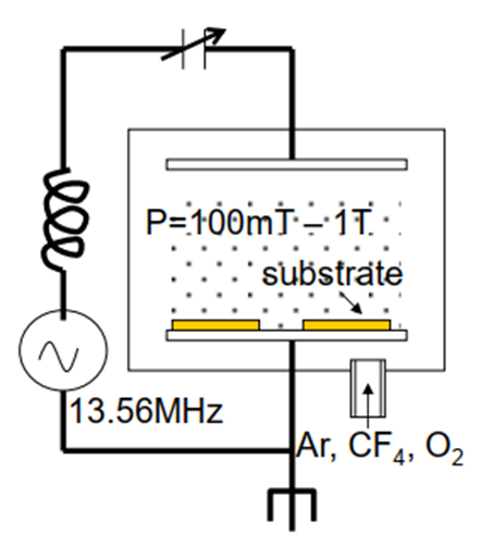 |
| Figure-3: Plasma etching setups |
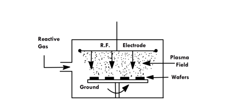 |
| Figure-4: Plasma etching process in semiconductor fabrication |
Both top and bottom electrodes are equal in size and parallel to each other. Bottom electrode holds the wafer and it is grounded. Due to the application of RF voltage and high pressure (P = 100mT to 1T) a plasma is set up between the two electrodes. High energetic electrons react with gas molecules and give various reactive species, neutral species and ions. Neutral species provide chemical etching and ions provide physical etching and a combination of reactive species and ions provides Ion Enhanced Etching.
We will discuss the prevention techniques of the Antenna effect in the next article.
Thank you.
This comment has been removed by a blog administrator.