Before starting this article, I would like to say this topic is highly sensitive and we are not supposed to reveal any foundry data. So Instead of making comments on any data which you know and I have not given here, you may mail me along with the reference link. The purpose of writing this article is only to make aware to new people who are preparing to enter into VLSI industry in an easy way.
Kindly note that none of the data is being added from our side in this article which is not available in the public domain. You will notice that many fields I have left blank intentionally, which you may know but the foundry has not reviled those data in the public domain.
So this article is just a collection of various data available on different websites instead of any data from my side. I will provide all the references at the end of this article, from where I have collected this information. I took all the care to maintain confidentiality but if anything you found is not appropriate to publish, please let us know through email.
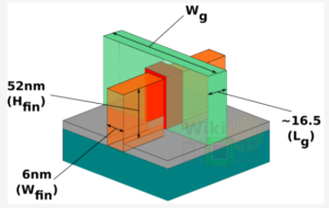
Below image may help you to understand various parameters of FinFET. This image is taken from https://fuse.wikichip.org/news/2408/tsmc-7nm-hd-and-hp-cells-2nd-gen-7nm-and-the-snapdragon-855-dtco/
 |
| Figure: FinFET structure and dimensions |
| S.N | Parameters | 7nm | 16nm | 28nm | |
| A. | Transistor wise | ||||
| 1 | Transistors | 4th Gen FinFET | FinFET | Planner MOSFET | |
| 2 | Gate Length (Lg) | 16 nm | 34 nm | 24 nm | |
| 3 | Fin Width (Wfin) | 6 nm | NA | ||
| 4 | Fin Heigth (Hfin) | 52 nm | 37 nm | NA | |
| 5 | Fin Pitch (Pfin) | 30 nm | 48 nm | NA | |
| 6 | Contacted Poly Pitch (CPP) | 57 nm (HD) 64 nm (HP) |
90 nm | 117 nm | |
| 7 | W effective | 3.66 | |||
| 8 | Minimum Metal Pitch (MMP) | 40 nm | 64 nm | 90 nm | |
| 9 | Standard Cell Height | 240 nm (6T) | |||
| 10 | Transistor Density | 91.2 M/mm2 | 28.9 M/mm2 | ||
| 11 | 6T SRAM bit cell size | 0.027 um2 | 0.074 um2 | 0.127 um2 (HD) | |
| 12 | Contact Trench Fill | Cobalt | Tungsten | ||
| 13 | Opertating Voltage | 750 mV | 800mv and 1V | ||
| B | Metal wise | ||||
| 14 | Total Metal Layers | 17 | 10 | ||
| 15 | Double Patern Layers | 7 (Fin, Poly, M0, M1, M2, M3, M4) | |||
| 16 | Patterning | Fins (SAQP) Poly to M4 (SADP) Rest Single |
DP | ||
| 17 | DUV/EUV | 193nm DUV + 13.5nm EUV | 193nm DUV | 193nm DUV | |
| 18 | Via Pillers | Yes | No | ||
| 19 | PG Routing | Dual M1 PG Structure | |||
| C | General | ||||
| 20 | Mass Production Year | Q2 2018 | 2015 | Q4 2011 | |
| 21 | Speed Improvement | 30%, comapre 16nm with same power | |||
| 40% , compare to 28nm with same power | |||||
| 22 | Power Reduction | -55% compare to 16nm with same speed | |||
| -55% compare to 28nm with same speed | |||||
| 23 | Density | 3.3X compare to 16nm | |||
| 24 | Cut metal | Area reduction through Cut metal layers. Routers are cut metal aware |
|||
Reference
https://en.wikichip.org/wiki/7_nm_lithography_process
https://fuse.wikichip.org/news/2408/tsmc-7nm-hd-and-hp-cells-2nd-gen-7nm-and-the-snapdragon-855-dtco/
https://en.wikichip.org/wiki/16_nm_lithography_process
https://www.tsmc.com/english/dedicatedFoundry/technology/logic/l_28nm
https://en.wikichip.org/wiki/28_nm_lithography_process
https://community.cadence.com/cadence_blogs_8/b/breakfast-bytes/posts/tsmc2


Have a Deep N -well in lower nodes ?