
Placement is a very important stage of physical design where all the standard cells get placed inside the core boundary. Overall QoR of the design greatly depends on the fact that how well placement is done. You must have noticed that the placement stage takes quite a large runtime. Actually, the tool performs various steps in a sequence to complete the placement stage. In this article, we will try to understand what are the important steps and the order in which the EDA tools perform to complete the placement stage.
Placement is the process of placing the standard cells inside the core boundary in an optimal location. The tool tries to place the standard cell in such a way that the design should have minimal congestions and the best timing. Every PnR tool provides various commands/switches so that users can optimize the design in a better way in terms of timing, congestion, area, and power as per their requirements. Based on the preferences set by the user, the tool tray to place and optimize it for better QoR. Placement does not place only the standard cells present in the synthesized netlist but also places many physical only cells and adds buffers/inverters as per the requirement to meet the timings, DRV, and foundry requirements. Here are the basic steps which the tool performs during the placement and optimization stage.
placement steps:
- Pre Placement
- Initial Placement / Course Placement / Global Placement
- Legalization
- HFNS (Hign Fanout Net Synthesis)
- Iteration for Congestion, Timing, DRV, and Power Optimization
- Multibit flop conversion
- Timing optimization iterations
- Scan-Chain Reorder
- Tie Cell insertion
- Save Design
1. Pre Placement:
 |
| Figure-1: Pre-placement step |
Before starting the actual placement of the standard cells present in the synthesized netlist, we need to place various physical only cells like end-cap cells, well-tap cells, IO buffers, antenna diodes, and spare cells. A typical view after preplacement has shown in figure-1. Why these cells are required to place and how do we place them has been discussed separately in this article. Here we will focus mainly on the placement steps of standard cells present in the synthesized netlist.
2. Initial Placement / Global Placement / Course Placement
 |
| Figure-2: Global placement before legalization |
Once the pre Placement stage has been completed, We can start the placement of standard cells but before that, we have to provide all the correct placement and optimization settings that we want to be applied while the tool does the placement and optimization. These settings could be like partial placement blockage or density screen setting, bound or region creation, cell/instance padding, path_groups and effort, enabling the early clock flow (ECF) in case of innovus, enabling the extreme flow, enabling the useful skew, global congestion effort, global timing effort, power effort, Multibit flop conversion and many more.
After providing all these placement settings we can call the placement command (place_opt_design in case of innovus). The tool first does the global placement in which the tool determines the approximate location of each cell according to the timing, congestion, and multi-voltage constraints (in the case of innovus Gigaplace engine is called in this step). Any pre-placed macros will work as a placement blockage. In this stage, the tool will not check any overlap of instances. A typical figure of global placement has shown in figure-2 where you can see that the standard cells are placed in an approximate location but without legalization.
3. Legalization
In the global placement stage, the instances are left with overlap. In this step, the tool will move the instances in nearby places to overcome the overlap. To match the proper power pins like the vdd pin of a standard cell should be on the vdd rail and vss on vss rail and for that if the fliping of instance is required tool also do the flipping. This process is called legalization. After this step, every instance should be placed in a legal location and there should be no overlaps. This step is also called refine placement.
4. HFNS (Hign Fanout Net Synthesis)
Initially, there are some nets which have very high numbers of fanout. We have a constraint of maximum fanout, so we need to distribute the sinks on nets to different drivers. The process of adding buffers and splitting the fanout is called high fanout net synthesis (HFNS). So In this step, all high fanout nets get synthesized.
5. Iteration for Congestion, Timing, DRV, and Power Optimization
In this step tool first, do an early global route and estimate the routing overflow/congestions in the design. The tool tries to initially minimize the congestion in this stage. Next, the tool starts the RC extraction to calculate the delay for setup analysis. The tool tries to minimize the setup WNS and TNS in this step. Similarly, the tool also tries to minimize the DRV and Power in this stage.
6. Multibit flop conversion
If the user enables the multi-bit flip flop conversion in the flow then the tool will first check the available multibit flops in the library. (You can read more about multi-bit cell here) The tool considers the criticality of timing associated with a single bit of flop and the user constraint set for multi-bit conversion and based on the constraints the tool converts the single-bit flop into multibit flops.
7. Timing optimization iterations
This is a long step in which the tool tries to minimize the WNS and TNS of each path group in various iterations. There are several iterations required to get a minimum WNS and TNS depending upon the effort set and initial WNS number. In case the result is not good after this stage, we can further run incremental optimization for timing. Similarly, for congetion, we can run congestion repair followed by incremental optimization to get a better result. But these additional steps will increse the run time.
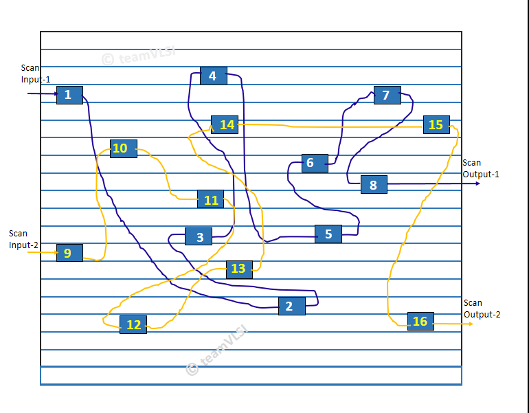
8. Scan-Chain Reorder
 |
| Figure-3: Scan Chain before placement |
Scan chain stitching has been done arbitrarily in synthesis. After placement and optimization, we have a location for each scan flops so it needs to be reordered for better routability. The tool performs a reordering of the scan chain in this step which is good for both timing and congestions.
 |
| Figure-4: Scan chain after placement |
 |
| Figure-5: Scan Chain after Scan chain reodrder |
9. Tie Cell insertion
There are some unused inputs of logic gates in the netlist which is tied to either vdd or vss. We can not leave any inputs of the standard cell as floating, it must be tied either vdd or vss. Connecting an input of logic cell that is the gate of a transistor directly to vdd or vss is not recommended and for that, we have tie high and tie low cells in the library. (You may watch this video on tie cells for more details). So In this step tool places tie high and tie low cells which is basically a single output logic cell, and it connects the input of the logic gate which needs to connect vdd or vss respectively.
10. Save Design
Finally, we save the database and we will use this database in the next stage, that is in the clock tree synthesis.
Helpful
What is Placement Attributes ???
Thanks Raji. Happy learning!!!
very helpful but it will be much better if you explained each term with images .