

The flip flop is the most commonly used sequential element in any ASIC design, especially the D-type flip-flop. In the D flip flop, the D indicates delay, which means the output is a delayed version of input D. Whereas a latch is the simplest and a basic sequential element. In general, there are two latches used to make a flip flop. the flip-flop is sensitive to clock edge and the latch is sensitive to clock level. The following section will explain the internal structure and operation of flip flops and latch. In this article, we will limit our discussion to only d type flip flops and d type latch which are most common in ASIC design.
Schematic of the latch and flip-flop
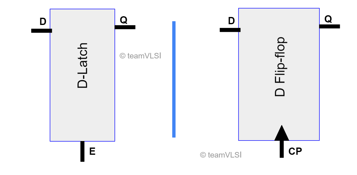
The simplest design latch and flip-flop both are having 3 pins, One input data pin (D), one input clock/enable pin (CP/E) and, one output pin (Q). There could be a set and reset pins also but here for simplicity we are not including those in our discussion. The symbolic representation of a latch and a flip flop has been shown in figure-1.
 |
| Figure-1: Symbolic representation of Latch and flip-flop |
In figure-1, the symbol of a posotive level sensitive d-latch and a positive edge triggered d flip-flop has shown. In negative latch and flip-flop only a dot appears before the E/CP pin. At a high level, we can think that latch and flip flop in terms of 2:1 multiplexer. A latch can be realized using a 2:1 multiplexer whereas to realize a flip flop, two multiplexers are required. Figure-2 showing the architecture of positive level sensitive d-latch and a positive edge triggered flip flop in terms of multiplexers.
 |
| Figure-2 : A positive d-latch and flip-flop using multiplexer |
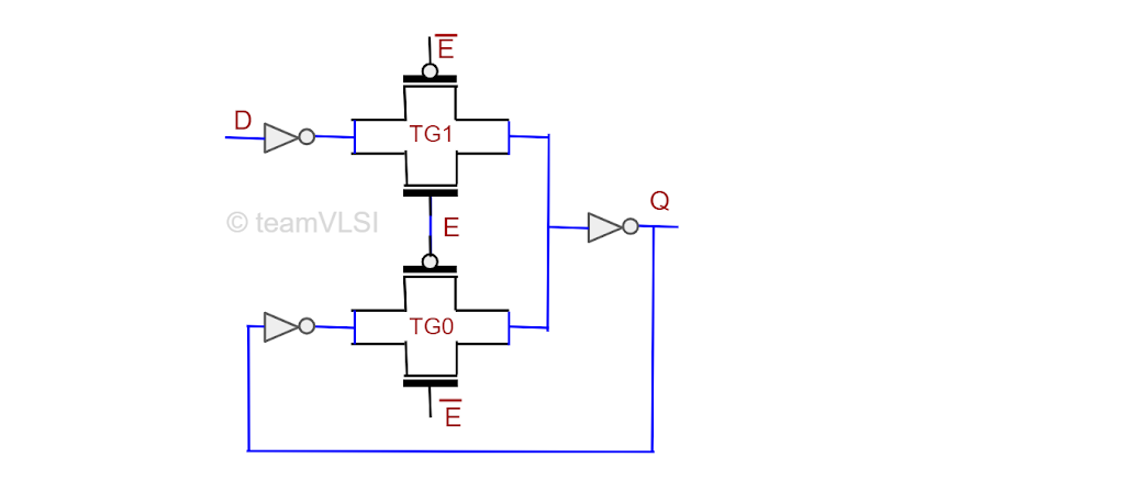
In a positive level sensitive latch the output is fed to I0 input of multiplexer as shown in figure-2. In same way in a negative level sensitive d-latch the output Q is fed back to input I1. A positive edge triggered d-flip flop is made of two negative level sensitive d-latch connected back to back. In case of negative d flip flop two positive level sensitive d-latch would be required. If we dive deep inside the multiplexer and go to the transistor level, we will find the transistor level schematic of a positive level sensitive d-latch and positive edge triggered d flip-flops as shown in figure -3.
 |
| Figure-3.a : A positive level sensitive d-latch using transmission gates |
 |
| Figure-3.b: A positive edge triggered d flip-flop using transmission gates |
A 2:1 multiplexer is made of two transmission gates and a transmission gate is made using a pMOS and an nMOS transistor as shown in the above figure. A latch is having two transmission gates in which the input of one transmission gate is connected to the output. A flip flop is made of two latches (that is four transmission gates) connected back to back as shown in figure-3. From the above figure, it is clear that a flip flop is having more transistors (double) as compare to a latch and hence a flip flop is having double the area as compared to the latch. The understanding of the working of latch and flip-flop is the most important part which will be discussed in the next section.
Working of a d- latch
The working of a positive level sensitive d-latch only is discussed here with the help of input and output waveform. The working of flip-flop will be discussed in the next section.
 |
| Figure-4: Input-Output waveform of latch |
There are two transmission gates are used in a d-latch. In case of a positive level sensitive d-latch the output is feedback to the input of TGO transmission gate. Transmission gates are made of a nMOS and a pMOS as shown in above figure and it is being controlled by the enable signal E which is actually the clock signal. When the enable signal is high, the nMOS and pMOSof TG1 is in on state and at the same time, both transistors of TG0 are in off state and vice-versa happens when the enable signal is low. There is a direct path established from pin D to pin Q when the Enabe signal is high and it is called latch is in transperent state. But when enable signal goes low, TG1 gate is in off state and a feedback loop is established between Q to input of TG0 which insures that there is no change in output Q irrespective of changes in input pin D, which is termed as latch state. Figure-5 shows when the latch is transperent and when it is latched through the waveform.
 |
| Figure-5: Working of a positive level sensitive d latch. |
The working of a positive level sensitive d-latch is straight forward, it keep passing the input D to Q when its enable signal E is high and and it keep the output Q unchanged when enable signal is low. Same can be seen in figure-5, only output changes when input changes and enable signal is high.
Working of a d flip-flop
In a positive edge triggered d flip flop, there are two negative level sensitive d latch connected back to back and the second latch is having inverted enable signal as compare to first latch. This inverted enable signal to second latch makes sure that both the latch never goes transperent or latched state simultaneously. A typical input output waveform has shown in figure-6 for better understanding.
 |
| Figure-6: Input output waveform of a positive d flip-flop |
Lets consider the the case when the clock signal is low, the first latch is transperent and input D is transmitted up to QM point. But at the same time second latch will be in latched state because it gets inverted clock signal so the output Q is latched with QM. There is no chance the outupt Q will get changed in this duration.
The next moment when clock signal transits from low to high, the first latch will go from transperent mode to latched mode and second latch will go from latched mode to transperent mode. So during the clock transition from low to high, whatever signal is sampled at QM previously gets transferred to the output Q.
The next moment when clock signal goes to high, there is not transfer of input signal D anymore and Wahtever signal previously samples at QM will be available at output Q.
The next moment when the clock signal transits from high to low, first latch will trasit from latched to transparent mode and second latch will transit from transparent to latche mode. So at this edge of clock transition there will be no change in output.
The operation of positive d flip flop can be summarized as, the output changes only at the rising clock edge and at this moment input D is trasfered to output Q and all other moment output is remain unchanged. So it is better in terms of avoid glitch as comapare to latch but more in area and more prone to process variation. For detailed operation and comparison please watch this playlist.
Thank you.