
We all know that all the input and output pins of a block must be constrained in order to enable the PnR tool to optimize those interface paths. How to constrain an input or output pin will be discussed in this article. We will also discuss what are the actual meanings of these constraints and how these constraints affect the timing analysis.
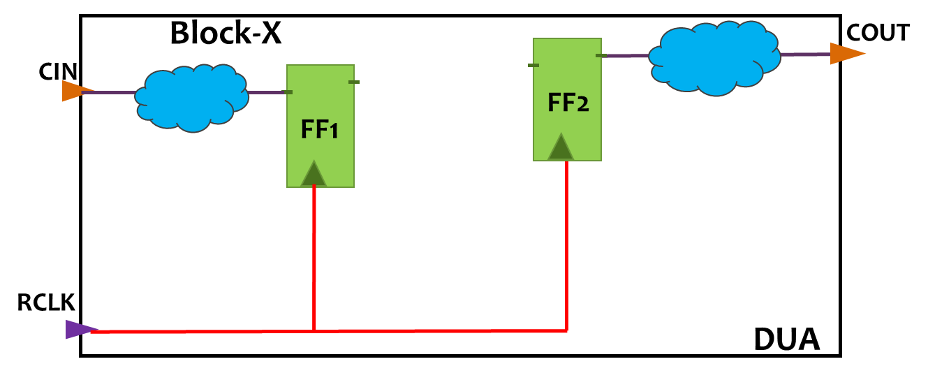
In the above figure, there are two timing paths shown, one is from CIN to FF1 and other is from FF2 to COUT. The path from CIN to FF1 is called input to register (In2Reg) path whereas the path from FF2 to COUT is called register to output (Reg2Out) path. Any timing paths which are related to an input and output pins is called Interface timing path.
Input Interface:
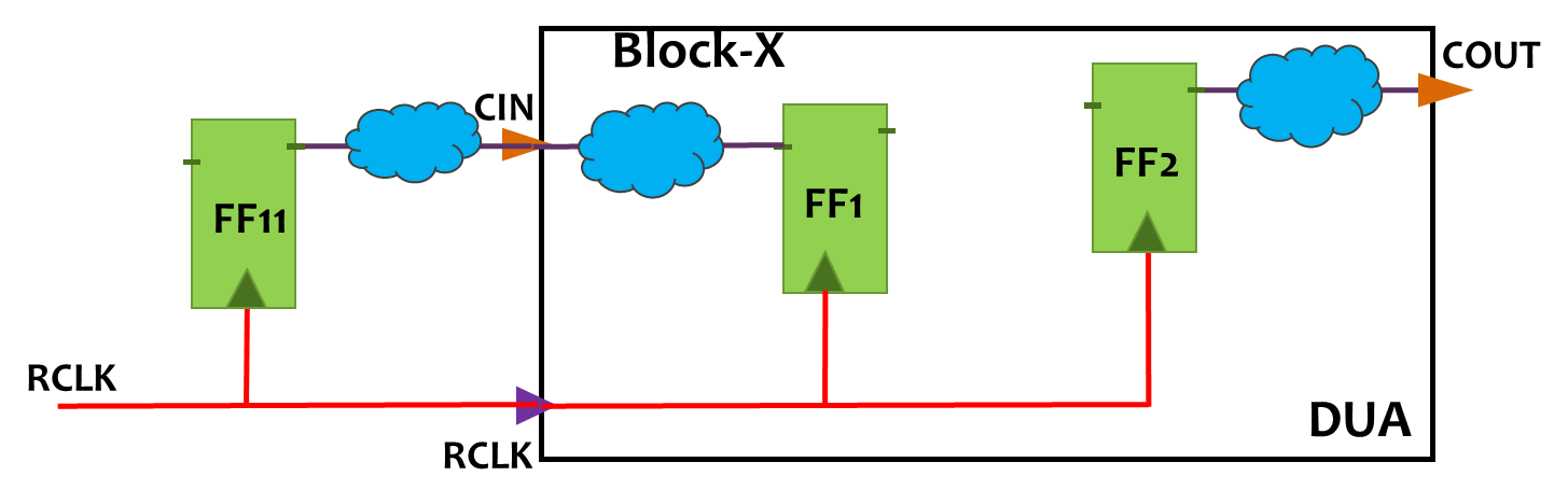
If we consider a block-level PnR implementation, the input to register path might be a part of the register to register path as shown in the above figure. Register FF11 is outside of the block but a part of the path from CIN to FF1 is inside the block. So in order to meet the timing of register to register path FF11 to FF1, we can divide this path into two parts.
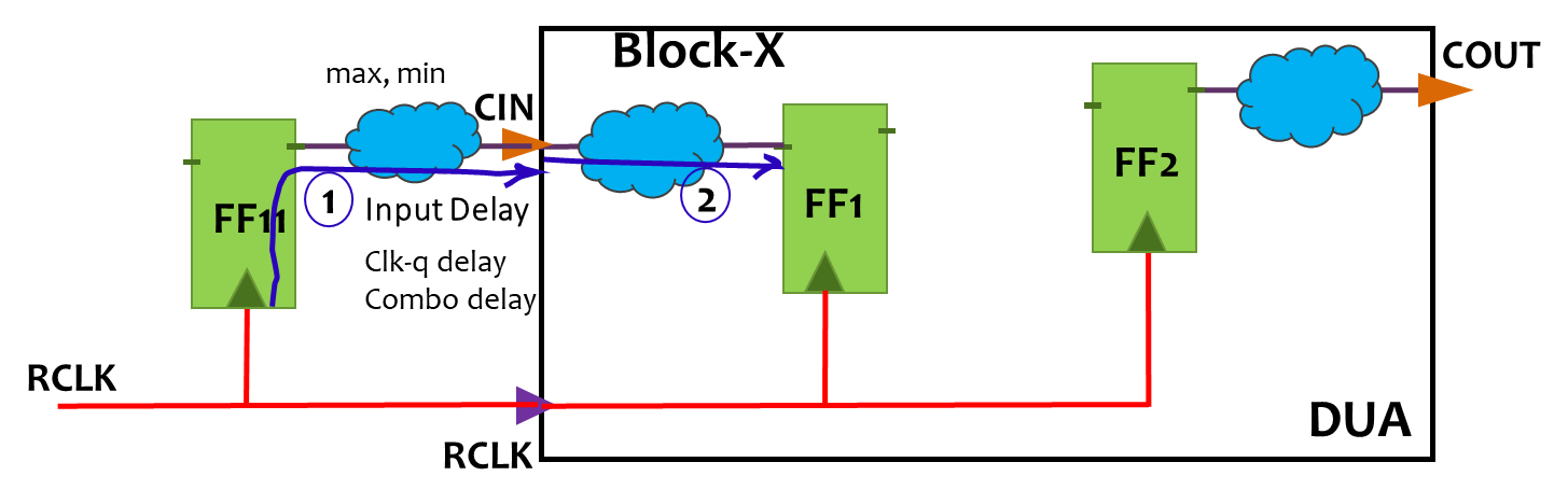
First part is the delay between the clock pin of FF11 to the input pin of block CIN and the second part is the delay from CIN pin to the D pin of FF1 as shown in the above figure. the first part is called input delay of the CIN pin. Since this path is out of the block so there is no timing information if this path can not be calculated by the tool. So we need to provide the delay of this part of the path as an input delay of pin CIN in SDC file. based on this input delay value PnR tool will estimate the timing margin from CIN to D pin of FF1 and optimize the path. On the block level, we need to close the timing from CIN to FF1 only that is Input to register path.
For Example,
let’s say the clock period is 1ns.
And for setup analysis, the data required time for the path FF11 to FF1 is 850ps.
Suppose the maximum delay of the path from the clock pin of FF11 to CIN is 550ps.
Then on block-level, for setup analysis, we have to close the remaining path that is from CIN to FF1 at 850 – 550 = 300ps.
Input delay path has also two parts, one is clock to q dealy of FF11 and other is a combinational delay from q to CIN. This path will have max and min delay, which will be used separately in the setup and hold analysis. So when we apply input delay we apply two delays, max input delay and min input delay. The command for applying this delay in the SDC file is as follow.
Setting Input Delay:
create_clock -name RLCK -period 1 [get_ports RCLK]
set_input_delay -max 0.55 -clock RCLK [get_ports CIN]
set_input_delay -min 0.45 -clock RCLK [get_ports CIN]
The above set of SDC commands will set the maximum input delay of 550 ps and minimum input delay 450 ps to CIN input pin. We can understand this in a more simple way that data will be launched from the CIN pin after the input delay. So more input delay means lesser time available to reach the data to capture flop FF1. A similar logic is applicable for hold analysis too.
Output Interface:

In block level, the register to output path from FF2 to COUT is a part of the complete path from FF2 to FF22 as shown in the above figure. Flip flop FF22 and the path from COUT to the FF22 is outside the block and this path can be supposed here a virtual path.

For Example,
let’s say the clock period is 1ns.
And for setup analysis, the data required time for the path FF2 to FF22 is 800ps.
Suppose the max delay of the path-2 from COUT to FF222 is 250ps.
Then on block-level, for setup analysis, we have to close the remaining path from FF2 to COUT at 800 – 250 = 550ps.
Setting Output Delay:
create_clock -name RLCK -period 1 [get_ports RCLK]
set_output_delay -max 0.25 -clock RCLK [get_ports COUT]
set_output_delay -min 0.20 -clock RCLK [get_ports COUT]
The above set of SDC commands will set the maximum output delay of 250 ps and minimum input delay 200 ps to COUT output pin. We can imagine this like there is a virtual flop outside the block and the delay from COUT pin to that virtual flop is output delay of COUT pin. Here output delay has explained with reference to setup analysis but a similar concept is applicable for the hold analysis too.
Thanks!
Nice conceptual explanation!
Thanks Priya, for appreciation.
Hi, even though the signal passes via cin to cout via flip flops we have to virtually assume that the input signal passes via a flip flop and reaches output via a flip flop, SO if we want to do timing analysis for combinational circuit still do we need to assume flipflop virtually in input and output