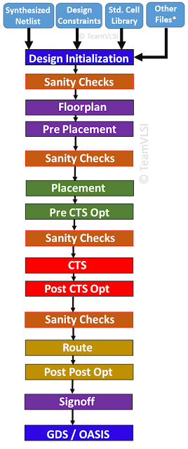
In RTL to GDS flow, Physical Design is an important stage. In physical design, synthesized netlist, design constraints and standard cell library are taken as inputs and converted to a layout (gds file) which should be as per the design rules provided by the foundry. Further, this layout is sent to the foundry for the fabrication of a chip.
This whole process of converting the gate-level netlist to layout is termed as physical design. In physical design, there are various stages of design, various mandatory checks in each stage and involved various analysis and verifications. In this article, we will see an overall flow of physical design and details of each stage, sanity checks, analysis and verifications will be covered in the coming articles.
Here is a basic physical design flow. There are some minor changes in this flow from company to company.
 |
|
|
PrePlacement Stage:
In Physical design, flow start with some set of input files and do the sanity check first once the design is loded into PnR tool. Sanity checks before floor plan are must in order to make sure that netlist, standard cell library and constraint are correct or not. After that floorplan stage starts where the macro placement is done. A good floorplan of design is a critical thing, it decides the overall quality of your design. If floorplan is not well it may lead to several issues in the next stages and it is quite possible that we need to change the floorplan and start again. In general, there are many iterations are required for a physical design engineer to get a quality floorplan. If a block is macro dominant and cell density is high than the floorplan stage is more critical. A good floorplan help to achieve a less congestion and good timing. How to do a good floorplan will be discussed in the other article.
Once the floorplan is done, we need to create the power plan followed by adding antenna diodes, well tap cells, endcap cells, decap cells. What are these cells and why we need will be discussed in the coming article. Generally, this step is called pre-placement stage. Once the preplacement is done we need to again perform a sanity check before the placement stage.
Placement Stage:
After the preplacement, we do the placement where all the standard cells are placed and legalized. There are various steps placement stage which tool performs, these steps will be discussed on a later article. Once the placement is done we need to perform the optimization for better timing and congestions.
CTS Stage:
Before the Clock Tree Synthesis (CTS) stage the clock is ideal. CTS is a step in which clock is distributed to all the synchronous elements in the design. Before start CTS we need to do sanity checks that the inputs of CTS is proper or not. In CTS there are basically two steps first build a clock tree and then balance the skew of the clock tree. Quality of CTS is very important in order to meet the timing requirements. A separate article will be done on CTS. After CTS we need to analyze the quality of the clock tree, timing and congestion.
Route Stage:
Route stage comes once the Clock tree is built and routed. In routing, there are basically two stage global routing and detail routing. Power nets and Clock nets are already routed, In this stage, we need to route the data nets.
Signoff Stage:
Once routing is done we need to insert fillers cells followed by metal fill and then Power signoff, timing signoff, and physical verification. Once all these steps are done in final we stream out the layout in the form of gds or OASIS file which is called tapeout. A detail discussion on each stage will be on coming articles.
* In other files, you may require DEF file, Floorplan file, Power intent (UPF/CPF) file, Technology file, RC coefficient file etc
Thank you.
