Decap cells are basically a charge storing device made of the capacitors and used to support the instant current requirement in the power delivery network. There are various reasons for the instant large current requirement in the circuit and if there are no adequate measures have taken to handle this requirement, power droop or ground bounce may occur. These power droop or ground bounce will affect the constant power supply and ultimately the delay of standard cells may get affected. To support the power delivery network from such sudden power requirements, decap cells are inserted throughout the design. In this article, we will discuss the structure and layout of decap cells, need of using decap cell and placement of decap cells.
Schematic and layout of Decap cell:
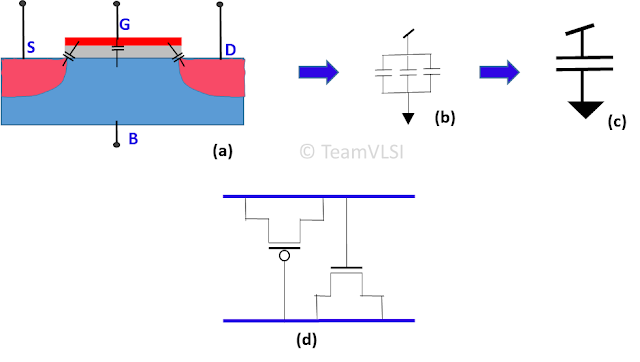
There could be various ways to make capacitors out of MOS transistors but the must widely used structure is shown in the figure-1.
 |
| Figure-1: MOS Capacitances and Decap cell schematics |
Figure-1(a) shows the various capacitances inside the MOS transistor and it if we connect the source, drain and body terminal together then all these capacitance will configured as a parallel capacitance as shown in figure-1(b) and a single equivalent capacitance as shown in figure-1(c). Figure-1(d) shows a decap capacitor schematic using a pMOS and an nMOS transistor. From this schematic, we can say that the capacitance due to nMOS and pMOS will be in parallel and get added to form a big capacitor. Figure-2 shows the layout of a simplest decap cell.
 |
Figure-2: Layout a decap capacitor |
Source and drain of pMOS transistor shorted together and connected to VDD and the Gate is connected to VSS. Similarly, the source and drain of the nMOS transistor are connected to the VSS and gate is connected to VDD.
Use of Decap cell:
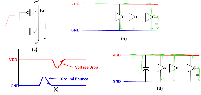
In the operation of CMOS logic, there is a region of input transition where both the nMOS and pMOS is conducting together as shown in figure-2(a). A large short circuit current Isc will flow for that instant. If a large number of such cells are placed together and switching together, a large current will be required as shown in figure-2(b). This large current requirement may drop the VDD or may increase the ground voltage which is called voltage droop or groud bounce as shown in figure-2(c).
 |
| Figure-2: Need of Decap cell |
Voltage droop or ground bounce may result in the change in the delay of connected standard cells. As the delay is proportional to the supply voltage. Change in delay may further affect the timing of design and if the supply voltage drop is high, the functionality of the standard cell may get affected. So to support the power delivery, we add the decap cells. Decap cells work as charge reservoirs and support the power delivery network and make it robust as shown in the figure-2(d).
Placement of Decap cell:
Decap cells are placed generally after the power planning and before the standard cell placement, that is in the pre-placement stage. These cells are placed uniformly throughout the design in this stage. Decap cells can also be placed in the post route stage also if required.
The only problem with decap cells is that these are leaky and increases the leakage power of design, so must be used judiciously.
Thank you.

Nice blog. I have watched your Youtube video too. I have few questions regarding it. Can you share some insights on how many decaps we need to place in the Microprocessor based chip? Where do you place decaps in microprocessor chip? Can you make a video on chip level placement of decap cells?
You should run a IR analysis on the design with power rail and see the hotspots and then place the decap cell.
Thanks Sukanta,
Sorry for the late reply, somehow I missed your comment.
Numbers of required decap can not be calculated straight forward. A common approach is do the IR analysis and based on IR violations and hot spots place the decaps. Some time a power hungry cells also need decap around it. So a through IR analysis is required for this.
Yes, Exactly!
Thanks for your reply. Yes, I am aware about that we need to perform IR drop analysis (or power grid analysis) to locate the hotspots. However, I needed more information about the decaps/decap cells that are used in the real designs. How are different parameters of the decap cells calculated etc?
Thanks for your reply. Yes, I am aware about that we need to perform IR drop analysis (or power grid analysis) to locate the hotspots. However, I needed more information about the decaps/decap cells that are used in the real designs. How are different parameters of the decap cells calculated etc?
I think you can check in apl cdev file
DC link capacitors This particular is usually apparently essential and moreover outstanding truth along with for sure fair-minded and moreover admittedly useful My business is looking to find in advance designed for this specific useful stuffs…