
In this article, we will discuss sources of On-Chip Variation (OCV) in VLSI, Why On Chip Variation occurs and how to take care of on chip variation in physical design. We will also discuss in very brief about the Advance On Chip Variation (AOCV) and Parametric On Chip Variation (POCV).
Background:
The final output which goes to the fabrication laboratory after physical design and signoff in the ASIC design cycle is the .gds (Graphical Design System) file. IC (Integrated Circuit) is fabricated on the silicon wafer, based on this final gds data. A big silicon wafer is divided into the various small die and each die contain an individual IC. After wafer-level testing, we cut and separate each die and do packaging of IC.
We have the same gds data for all the ICs in all die but the location of dia is different on the wafer. If the gds is same for all the die then ideally electrical characteristics of all the ICs should have the same. But practically it is not. The IC manufactured in different die has variation in their electrical characteristics. Figure-1 shows a silicon wafer and die on the wafer.
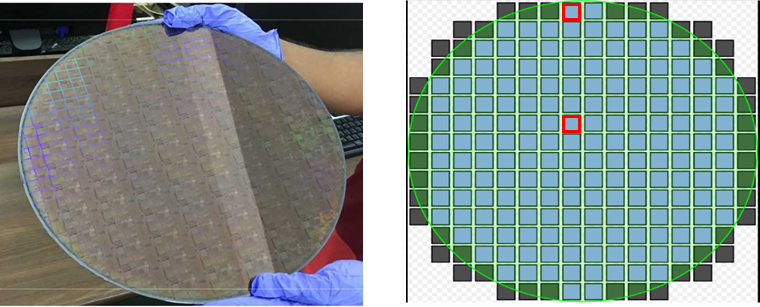 |
| Figure-1: Silicon wafer and die on the wafer |
For example, let us consider three dies at different locations on the wafer as shown in the figure-2. Die-1 is situated at the centre of the wafer, die-3 at the edge of wafer and die-2 in between the centre and outer edge.
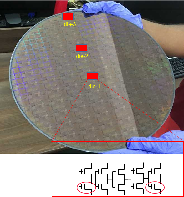 |
| Figure-2: Wafer, dies and transistors inside die |
So Inside a wafer, there are hundreds of dies and there is a variation in each dia and also in the lots of wafers. Or if we investigate more deeply we found that there are millions of transistors inside an IC and all the transistors inside a single IC are not similar. So there are variations in the characteristics of transistors even inside a single IC along with the die and lots. Now an important question comes, from where all these variations come? What is the root cause of these variations? And the answer is the fabrication process itself is the main cause of these variations. So let’s investigate the source of these variations.
Sources of Variations:
There are three major sources of variations, Process, Voltage and Temperature. These variations are collectively called PVT variations. We already do PVT analysis and take care of these variations while designing an ASIC, then why we need to take care of OCV separately? And the answer is, all the variations can not be taken care in PVT analysis. Some of them are predictable and can be modelled easily as the technology get matures but some of them are highly unpredictable and can not be modelled easily. Figure-3 shows the various components of the PVT and OCV variation together.
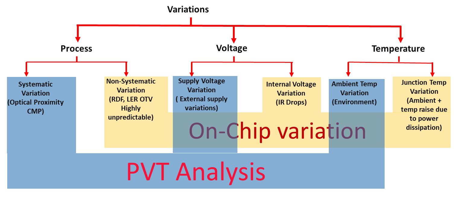 |
| Figure-3: Variation components under PVT and OCV |
In process variation, there are two types of variations one is systematic variation and other is a non-systematic variation or random variation. Systematic variations come due to Optical Proximity Corrections (OPC) or Chemical Mechanical Policing (CMP) which are predictable in nature and can be modelled in PVT variations. Non-systematic variations come from the Random Dopant Fluctuation (RDF), Line Edge Roughness (LER) or due to Oxide Thickness Variations (OTV) which are highly unpredictable and can not be modelled easily. Or we can say that these variations are random in nature.
In Voltage variation, one is due to variation in external supply voltage and other is internal voltage variation inside the chip. There is no ideal voltage supply and there is always 2-5% variations in supply voltage even after utmost care is taken in the supply voltage design. This type of variation is taken care in PVT but another type of variation is due to internal IR drops and it is not possible to model in PVT as it is random in nature and depends on the design. So we need to take care of such voltage variation in the OCV.
If we talk about temperature, then there is an ambient temperature on which the chip is operating and another temperature is the junction temperature of the transistors. junction temperature is the sum of ambient temperature plus the temperature raised due to power dissipation in the chip. Junction temperature is always much greater than the ambient temperature and the characteristics of any transistors majorly depend on the junction temperature. Ambient temperature can be taken care in PVT but for the junction temperature variations, we need to take care in OCV.
Let’s discuss more all these variations.
I. Process Variations:
The drain current of an nMOS transistor in the linear region can be defined as

Where Id is the drain current, μn is the mobility of electrons, ∈ox is the permittivity of silicon oxide, tox is the oxide thickness, W is the width of transistors and L is the gate length of the transistor as shown in figure-4.
 |
| Figure-4: Terminals and schematics of a MOS device |
In the drain current equation, the factors which are dependent on the fabrication process are:
Gate Oxide Thickness (tox)With of transistor (W)Length of the transistor (L)and Threshold voltage of Transistor
So if any of the factors mentioned above varies during the fabrication process, It will affect the drain current. The delay of a cell is dependent on the drain current so due to process variation, the delay of a standard cell is going to vary. Now see some example, how these parameters can get affected during the fabrication process. Figure-5 and Figure-6 show the length and width variation associated with the photolithography process.
 |
| Figure-5: Optical Proximity Correction |
Optical Proximity Correction (OPC) is a process which is applied to the layout before mask generation in order to get better replication of layout on the wafer. In this process generally, the corner edge is of layout extended to get a better yield. A general photolithography flow has shown in figure-6.
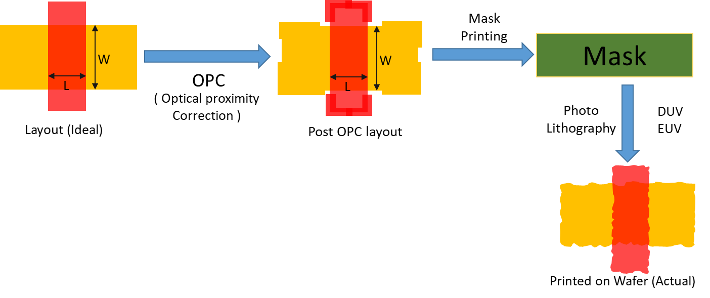 |
| Figure-6: Photolithography flow |
A photolithography process is a non-ideal process and it is very hard to print the exact layout on the silicon wafer. So there are variations in the dimension of actual layout and printed geometry on the wafer.
Process variation generally includes:
So, in conclusion, there are many factors and high chances of variation while fabrication of a chip and these can lead the vary the delay of the standard cells.
II. Voltage Variations:
The external voltage variation is taken care in the PVT but there could occur internal voltage variation in your chip based on the design. There could occur IR drop in your power delivery network which may lead to variation in available voltage to operate a cell.
Power comes from the power pads/ Bumps and distributed to all standard cells inside the chip through the metal stripes and rails which is collectively called the power delivery network (PDN) or power grid. Distance between the power pad and standard cells could not be the same for all the standard cells. So there will be a variation of available VDD for the standard cells depending on the design. Delay of a cell is dependent on the available VDD, If VDD is less delay will be more.
III. Temperature Variations:
Transistors characteristics are strongly dependent on the junction temperature. Ambient temperature is taken care in PVT as per the application of ASIC. But junction temperature is dependent on the design of the chip. Power dissipation inside the chip could raise the temperature of nearby junctions and it could affect the performance of the entire chip.
Sometimes there is also the formation of local hotspots based on the placement density and power requirements of cells which affects the temperature of the junction and ultimately lead to the variation in current and delay of cells. Junction temperature is the sum of ambient temperature and the temperature raised by the power dissipation of cell. This whole thing is not predictable and can not be taken care in PVT so we have to take care of these variations in OCV.
Effects of On Chip Variation:
On Chip Variation is could lead to post-silicon failure if it is not taken care while designing the ASIC. Consider a case where there is an increase in delay in the data path or increase of delay in launch clock path or there is a decrease of delay in the capture clock path due to OCV. In all cases, there might be a setup time violation due to OCV. A similar case could also occur for the hold time. A proper timing closure chip could violate the timing and fail if we don’t take care of OCV.
How to take care of OCV:
To take care of OCV we need to add some pessimism in the timing of standard cells. We basically apply ±x% of additional delay to all the standard cells. Which is called OCV derate.
OCV derate factor:
Derate factor is a very simple approach to take of on chip variation. A fixed derate factor is applied on throughout the design. So that in case of any variation occurs will not cause the failure of the chip. But it added too much of timing passimism which leads to difficulties in the timing closure, especially in the lower nodes.
So the industry has moved to different concepts from the fixed derate to distance and depth based derate which is called Advance On Chip Variation (AOCV). As the technology node further shrank more, AOCV also is not a good option and further Parametric On Chip Variation (POCV) evolved. We will discuss OCV, AOCV and POCV in another article. In short, we can say that as we moved from OCV to POCV timing pessimism reduced.
Thank You!
Excellent article @TeamVLSI. All the information in very somple and effective manner…Thank you so much for providing quality content
Thanks a lot and it's my pleasure that you liked it.
Happy learning!
Thank you for sharing this article. I found it very useful and will certainly share it with others.
Polished silicon wafers
Thanks mike!
thank you team vlsi for such wonderful article
Glad that you liked it. Happy learning…
Great Article!
Please when the new article comes out, link it in the comments, thanks!
Hi Karim,
You can provide your email address in email subscription section (top right) it will deliver the article in your email and follow the article for updates.
thanks !! it 's great article.
Welcome! Happy learning!
Excellent overview on OCV!!
The best Explanation on the internet about On chip Variations
Thanks a lot @Samantula Durgaprasad!
These comments really fuel up us. Keep help to reach the post who really need this.
Thanks