Latch-up issue in CMOS Logic | Latch-up effect in VLSI
Team VLSI
What is a latch-up issue in CMOS design?
In the simplest way, the latch-up issue can be defined as a formation of a direct path from VDD to GND terminal in the design, which will cause a huge current flow between the power and ground terminal.
Latch-up Formation:
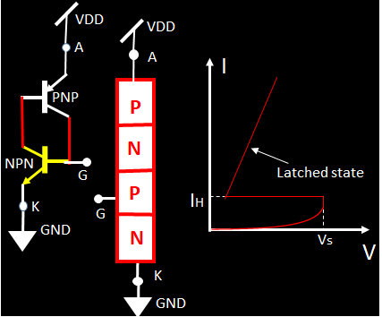
Inside a CMOS (Complementary Metal Oxide Semiconductor) circuit, two parasitic BJT (Bipolar Junction Transistors) get formed and connected in such a way that these BJT form a PNPN device or SCR (Silicon-Controlled Rectifier) or Thyristor. Formation of the PNPN device is shown in the figure below.
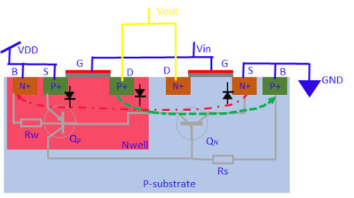
As shown in the above figure, a pMOS device is formed inside a nwell and a nMOS device is formed on the p-substrate region. If we see the region below the source or drain of the pMOS device, source or drain is formed with P+ implantation then nwell come and bellow the nwell there is p-substrate. So a parasitic PNP BJT formed here, whose emitter is the source of the pMOS, the base is the nwell and collector is p-substrate. In a similar manner a parasitic NPN BJT has formed near the nMOS device, whose emitter is the source of nMOS , the base is the p-substrate and collector is nwell.
Both this BJT are connected to each other in such a way that they form a PNPN device. The base of PNP BJT is connected to the collector of NPN BJT and base of NPN BJT is connected to the collector of NPN BJT.
A PNPN device is normally in OFF state and there are minimal current or no current flow through it. But once the PNPN device is get triggered by its gate signal, a large current starts to flow through it and it continues to flow even if the gate signal removed. The figure below shows the terminals of the PNPN device and its characteristics.
Technically latch-up is the phenomena of activating the parasitic BJTs in a CMOS circuit which forms a low impedance path between the power and ground terminals. This low impedance path draws a large current and heats up the IC (Integrated Chip) which cause permanent damage of IC.
Latch-up Triggering:
PNPN device formed inside the CMOS can be triggered by various means. Once the PNPN device is triggered by any means, the latch-up event will start. Some of the main reasons are as below.
Noise at the output terminal
ESD (Electrostatic Discharge) event
Ionizing radiation
Consider the above figure and suppose the output voltage has gone beyond the VDD due to noise, then it will forward bias the transistor between drain terminal and nwell of pMOS. Once this junction is forward bias, P+ region will start injecting hole to nwell, and these holes will be collected by body contact of nMOS as it is connected to GND. So this event will start flow of current from the drain of pMOS to the body of nMOS. Due to the flow of above-mentioned current, there will be a voltage drop between the source terminal of nMOS and the substrate below it. It will forward bias the pn junction between substrate and source of nMOS. This will again start injecting electrons from N+ source to the substrate, which will be collected by body terminal of pMOS which is connected to the VDD and shown in red dotted line. So eventually a chain will start and next source terminal of pMOS and nwell will be forward bias. In this way both the BJT has turned on and latched up.
In a similar way, if vout goes below the VDD , first the junction between the drain of nMOS and substrate will be forward bias, and it will make the junction between the source of pMOS and nwell forward bias and again this will further make the junction between the source of nMOS and substrate forward bias and both the BJT will be turned on and latch-up will occur.
Once the latch-up occurred in CMOS design, lots of current start flowing directly from VDD to GND and will cause the failure of chip. So we must protect our chip from latch-up. In the next article, we will discuss the method to prevent the latch-up issue.